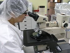
Our new laboratory facility located in Milpitas, CA offers a wide spectrum of materials analysis, micro-contamination analysis, and materials characterization using advanced analytical equipment and methods.
Micro-contamination Analysis and Identification
The SAS Laboratory provides micro-analysis of high purity electronic materials to sub-ppb levels in order to identify and characterize trace contamination in organic and inorganic samples. Test results of are always checked for accuracy by duplicate sampling at different times and conditions. Our policy is to use internal spiking and and internal standards on different concentrations to confirm the accuracy of results.
The highly skilled staff in our R&D department analyzes test results to determine the root cause of yield loss from micro-contamination and other process related problems. SAS scientists work directly with the customer's process and equipment engineers to achieve the most cost effective solutions to their problem. SAS may request additional samples to complete their studies and, if needed, will collect and evaluate samples at the customer’s facility.
SAS R&D is supported by a network of chemists, physicists, and engineers from academic institutions around the country. Depending on the nature of the assignment SAS is able to obtain expert advice to help solve virtually any problem.
Semiconductor Analytical Systems has performed many investigations into process issues related to semiconductor, solar and hard disk manufacturing. For example, we have identified the cause of contamination on ceramic elements in a CVD reactor, investigated and solved a dry etch process problem, and helped to achieve uniformity in a chemical purification process. SAS has successfully resolved these and many other process problems in a timely and cost-effective manner.
We welcome the opportunity to help you. Please contact us.
Analytical Testing Capabilties

 |
|---|
 |
 |
 |
 |
 |
 |
Analytical and Diagnostic Services

Semiconductor Analytical Services offers specialized testing services to support microelectronic, disk drive, solar, lithium battery and other high technology industries. Our experienced staff responds quickly to accomodate the specific needs of customers, and our rates are extremely competitive.
SAS respects the confidential nature of the work we perform and we take extra precautions to protect customer information and trade secrets.


Research and Development - Delivering effective solutions for over 30 years

Case Histories
CASE 1
Determining the cause of contamination on the surface of ceramic parts in a CVD reactor
CASE 2
Suppression of ionic contamination from an aqueous solution in an electric field
CASE 3
Determining the cause of isotropic profile in a dry etch process
CASE 3
Identify why a dry etch process failed to be anisotropic
A customer’s dry etch process was isotropic rather than anisotropic which was needed. The SAS analytical laboratory received a batch of silicon wafers to determine why this was happening.
The SAS laboratory did a preliminary analysis of the wafers and requested detailed technical information about the customer's process. After reviewing the all process parameters SAS determined the problem could be solved by using a pulse plasma reactive ion process instead of the continuous plasma process being used.
The SAS customer report stated:
In the continuous plasma process reactive ions such as CF3 are reacting with silicon to create by-products such as SiF4. The SiF4 ion must be removed quickly from the etching area or it will collide with another fresh CF4 ionic molecule, thereby changing the direction of the reactive ion beam to create an isotropic etch.
SAS recommended use of a pulse plasma instead of the continuous plasma being used. That way time is allowed to create a clear path for CF4 ions and a clean vertical line can be achieved. The customer changed to a Pulse plasma process and the problem was solved.


